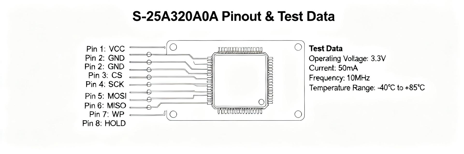
93C56 EEPROM Specs Breakdown: Pinout, Timing & Limits
In many legacy automotive, industrial, and embedded systems the 93C56 EEPROM remains a common on-board memory element. Engineers who understand the 93C56 EEPROM pinout, timing limits, and operating constraints reduce integration bugs and field failures.
Background & Key Specifications Overview
| Parameter | Specification Range | Notes |
|---|---|---|
| Memory Density | 2 Kbits | 2048 bits total capacity |
| Organization | 256 x 8 or 128 x 16 | Selectable via ORG pin |
| Operating Voltage | 2.7V to 5.5V | Varies by sub-model (L/C/V) |
| Clock Frequency | Up to 2.0 MHz | Dependent on VCC level |
| Write Endurance | 1,000,000 Cycles | Typical industrial rating |
Memory Capacity & Organization
The device is a 2-Kbit serial EEPROM typically organized as 256 × 8 or 128 × 16 words. Word width changes address length and command format; a 256×8 device uses 8-bit words and 8-bit addressing fields, while 128×16 halves address bits but shifts opcode framing—firmware must detect ORG pin state before issuing commands.
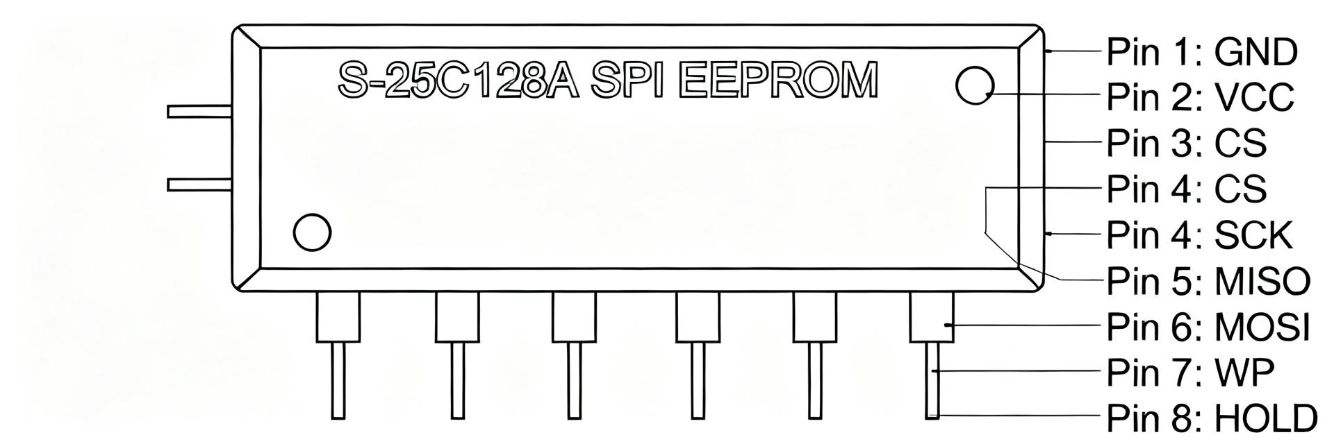
93C56 EEPROM: Pinout & Signal Descriptions
Signal-Levels & Recommendations
Logic thresholds follow the supply (VIL/VIH relative to VCC). Use 10 kΩ pull-ups on CS or CLK where bus-idle high is preferred; add 33–100 Ω series resistors for edge damping when clocking from faster MCUs. Place a 0.1 µF decoupling capacitor directly at the VCC pin.
Timing Parameters & Read/Write Cycles
Key timing specs include maximum clock frequency, tCH/tCL (clock high/low), data setup (tSU), and hold (tH). Violating setup/hold causes mis-sampled bits. Internal write cycles take a finite tWC (typically 5ms). After a write command, poll or wait tWC before the next access to prevent data corruption.
Interfacing & Command Set
The 3-wire serial protocol uses opcodes for READ, WRITE, ERASE, and EWEN/EWDS. Opcode frames vary by the ORG pin setting. In 8-bit mode, you must send 8 address bits; in 16-bit mode, the address field is reduced. Incorrect framing is the #1 cause of "offset" read errors in new firmware implementations.
Common Questions & Answers
How do I detect incomplete writes on a 93C56 EEPROM?
Read back the written word immediately after the write and compare it to the intended data. Use the device's status polling (checking the DO pin for a high state while CS is high) or implement a checksum across sectors and verify integrity after each write sequence.
Can I substitute an 8-bit and 16-bit organization interchangeably?
No. While packages may be pin-compatible, organization affects address width and opcodes. Substituting without firmware changes leads to shifted addressing and corrupted data. Confirm the ORG pin state (GND for x8, VCC for x16) before finalizing the layout.
What are quick checks when the device does not respond on the bus?
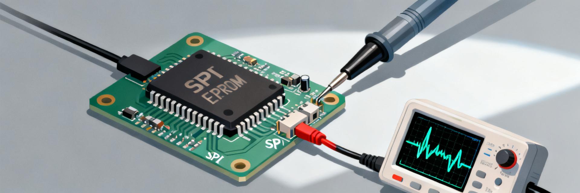
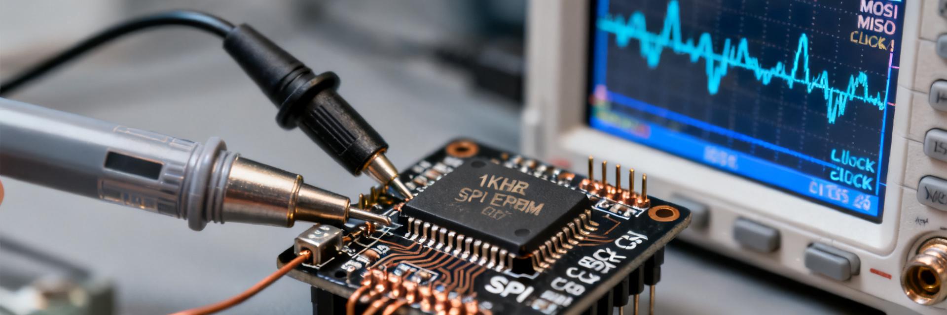
First verify VCC and GND continuity, then probe CS and SK (Clock) for activity. Confirm pull-up/pull-down resistors on the CS line. Capture a logic analyzer trace to ensure the opcode matches the organization selected by the ORG pin.
What is the maximum clock frequency for 93C56?
Typically up to 2MHz at 5V, though it may be lower (around 1MHz) at lower supply voltages like 2.7V. Always check the specific manufacturer datasheet for the exact speed-grade of your component.
Summary
Understanding the 93C56 EEPROM pinout, timing parameters, and operating limits prevents integration errors and field failures. Use the pinout map and timing margins to validate designs before production; always confirm the 93C56 organization (x8 or x16) before issuing commands or performing replacements.