S-25C160A0H-K8T2U3 Voltage & Timing Report: Pinout
The S-25C160A0H-K8T2U3 is a serial 16Kb EEPROM with a narrow low-voltage operating window and tight timing requirements. Key datasheet figures show supply and IO voltages plus access windows that drive decoupling, level-shift and tolerant-IO decisions. This report maps the voltages and pinout to speed validation during bench bring-up.
1 — Quick overview & key specs
Device class and core operating voltages are decisive for system integration. Designers must budget for standby, read and write IDD currents and honor absolute maximum voltages to avoid latch-up or data corruption.
| Parameter | Min | Typ | Max |
|---|---|---|---|
| VCC (Recommended) | 1.7 V | 3.3 V | 5.5 V |
| IO Domain | VSS | VCC | VCC + 0.3V |
| IDD Standby / Read / Write | ~1 µA | 2 mA | 10 mA |
| SCLK Frequency (max) | — | — | 5 MHz (@5V) |
2 — Voltage ranges & absolute maximums
VCC windows determine logic thresholds and IO tolerance. Validate guaranteed input low/high thresholds with a margin table and ensure power sequencing prevents inputs above the present VCC during ramp events.
| VCC (V) | Guaranteed VIL (max) | Guaranteed VIH (min) |
|---|---|---|
| 1.7 | 0.3·VCC | 0.7·VCC |
| 3.3 | 0.3·VCC | 0.7·VCC |
| 5.5 | 0.3·VCC | 0.7·VCC |
3 — Pinout breakdown: signal-by-signal
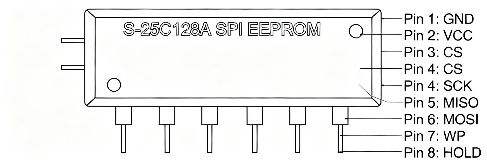
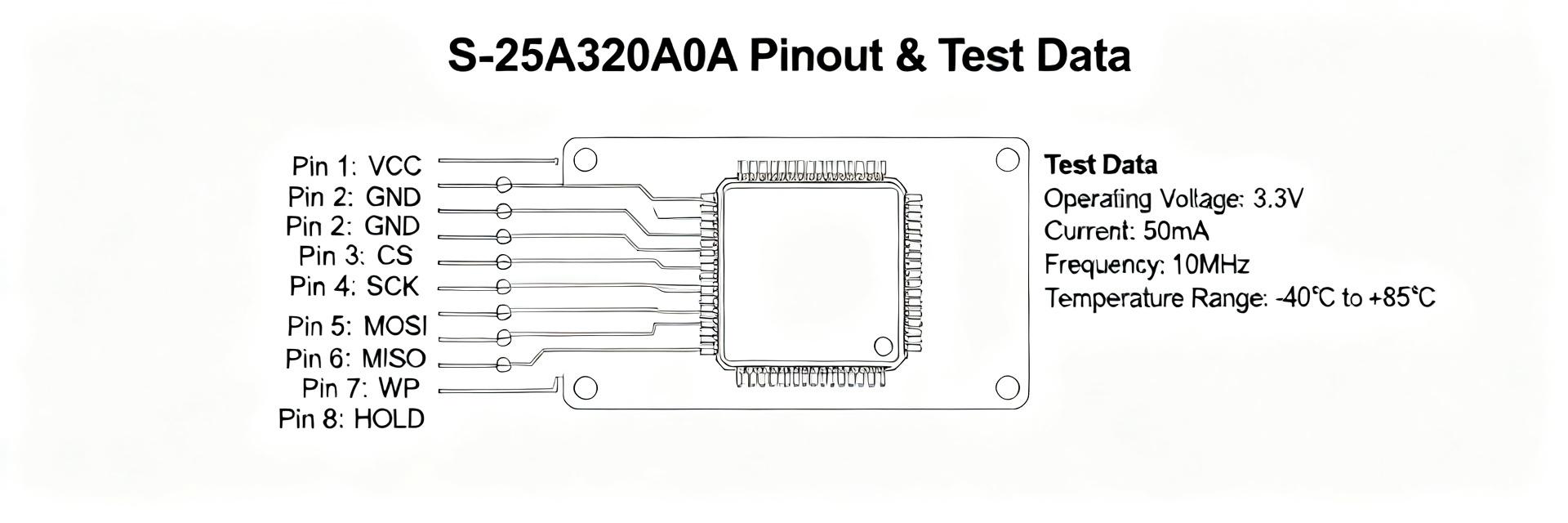
Clear pin definitions speed bring-up. The S-25C160A0H-K8T2U3 pinout assigns CS, SCLK, SI, SO, WP, VCC, GND and HOLD; idle states are defined in the datasheet.
| Pin | Signal | Do / Don't |
|---|---|---|
| 1 | CS/CE | Do: pull high; Don't: leave floating |
| 2 | SO/MISO | Do: tri-state when CS high |
| 3 | WP | Do: pull to VCC to disable protection |
| 4 | GND | Do: solid plane, multiple vias |
| 5 | SI/MOSI | Do: series 22–47Ω for signal integrity |
| 6 | SCLK | Do: controlled edges; Don't: long traces |
| 7 | HOLD | Do: tie high if not used |
| 8 | VCC | Do: decouple 0.1–1 µF at pad |
4 — Integration checklist & troubleshooting
A compact checklist reduces field failures. Key items include correct VCC decoupling, level shifters if IO domain differs, and CS/WP pull states.
- VCC Decoupling: Use 0.1µF X7R ceramic capacitors within 2mm of Pin 8.
- Timing: Implement a polling loop (status read with timeout) rather than fixed long delays for write cycles.
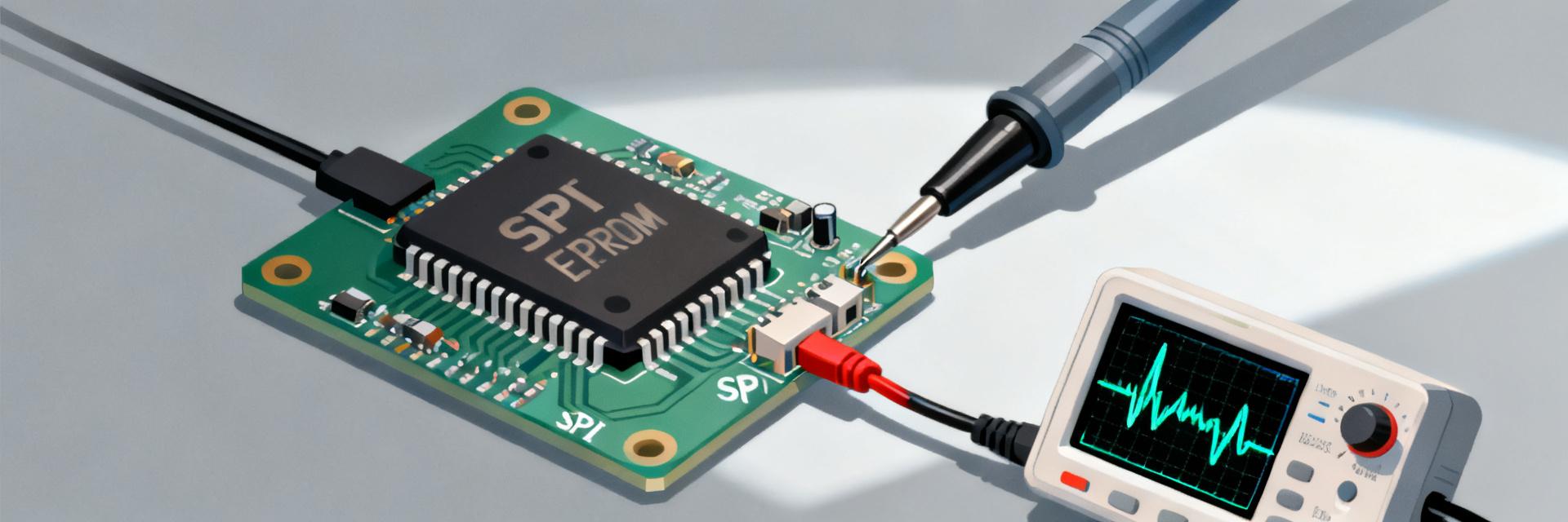
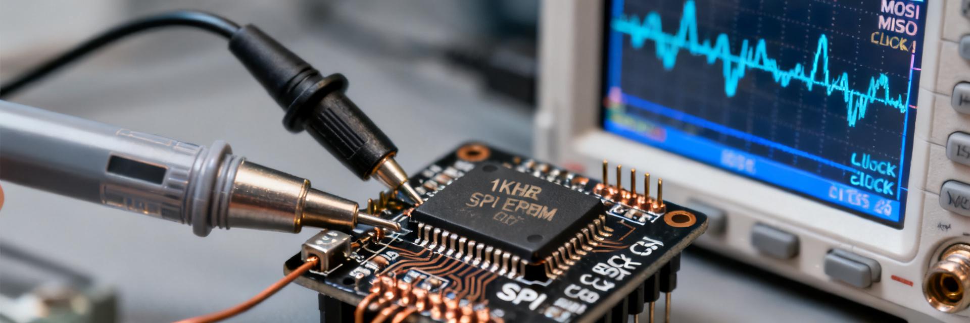
- Integrity: Capture CS, SCLK and SO simultaneously during bring-up to verify tACC.
FAQ
How to verify S-25C160A0H-K8T2U3 voltages during board bring-up?
Measure VCC at the package decoupling point under idle and during write; expect low ripple with a 0.1–1 µF cap within 1–2 mm. Verify IO thresholds relative to VCC and confirm no pin exceeds VCC + 0.5 V or drops below GND −0.5 V during power transitions.
What are quick checks for S-25C160A0H-K8T2U3 pinout and basic signal integrity?
Confirm CS default high, WP state matches intended protection, and SCLK edges meet slew and timing requirements. Probe CS, SCLK and SO simultaneously; look for valid SO after tACC and ensure no bus contention when VCC is absent or during reset sequences.
How to measure S-25C160A0H-K8T2U3 timing if writes appear unreliable?
Capture the write sequence with a high-bandwidth scope and mark tWC and status-poll intervals. Inject known-good patterns at reduced SCLK to separate timing issues from level problems; if tWC variance is large, increase firmware timeout and add verification reads after writes.
What is the proper handling of the WP and NC pins for S-25C160A0H-K8T2U3?
The WP (Write Protect) pin should be tied high to VCC to disable hardware protection or low to GND to enable it; never leave it floating. NC (No Connect) pins should be left electrically isolated from any signals to avoid internal parasitic interference.