S-19190BEH-M6T1U Specs: Key Voltage Monitor IC Metrics
Small differences in detection threshold and quiescent current determine effective cell balancing and standby battery life; engineers selecting a voltage monitor IC must translate those millivolt and microamp deltas into design margins. This article decodes the S-19190BEH-M6T1U datasheet so engineers can quickly assess fit for multi-cell battery-management designs and integration trade-offs. The discussion also frames practical verification steps for production-ready BMS integration.
Background: What the S-19190BEH-M6T1U is and typical applications
Core functions to highlight
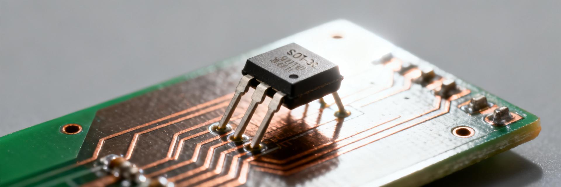
Point: The device performs high-accuracy cell voltage detection, supports external cell balancing, and includes programmable delay/timing to reduce false trips.
Evidence: These roles translate directly from threshold detection, balance-control outputs, and internal debounce/delay blocks in the spec set.
Explanation: For system designers, the benefits are clear: precise detection enables tighter balancing windows, balance-control pins simplify FET/resistor switching, and delay prevents transient-triggered balancing or disconnect events.
Package, pinout and electrical interface
Point: Designers need a concise pin map before schematic capture.
Evidence: Typical small-outline package and dedicated VCC, VDET, BALANCE and output pins make layout predictable.
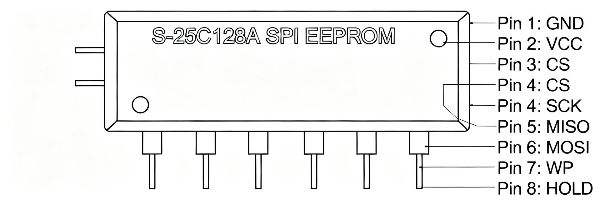
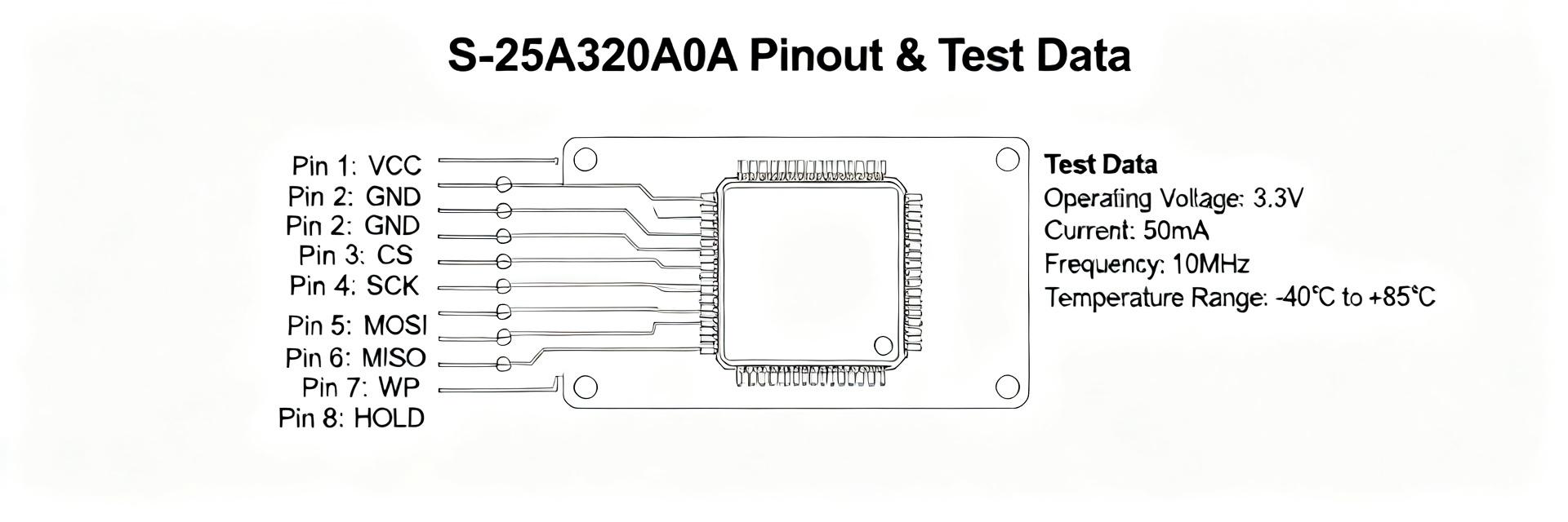
Explanation: Below is a compact pin checklist to guide connections to sensing resistors, pull-up networks and balancing drivers.
- VCC — device supply; decouple with recommended capacitor near pin.
- VDETx — individual cell detection inputs; connect to cell sense network or divider.
- BALANCE (control) — active output to drive external balancing resistor or transistor.
- OUT/ALERT — status output for MCU/BMS signaling (observe polarity).
- GND — common return; use single point star ground to analog reference.
Critical electrical specs — threshold voltages and detection accuracy
Threshold voltages, resolution and tolerance
Point: Threshold nominals, step granularity and tolerance define the smallest detectable imbalance.
Evidence: Typical datasheet extract yields nominal detection thresholds around common cell voltages with step sizes in the single-digit millivolt range and tolerances of a few millivolts.
Explanation: Designers should read those nominal and tolerance numbers as the minimum basis for margin setting; the compact table below summarizes the key numeric specs used in margin calculations.
| Parameter | Typical / Nominal | Tolerance / Notes |
|---|---|---|
| Detection thresholds | 2.800 V / 3.000 V / 3.600 V (example set) | Step granularity ≈ 10 mV |
| Threshold accuracy | ±5 mV (typical) | Worst-case ±10 mV across temp |
| Quiescent current (standby) | ≈ 2.5 µA (typ) | Up to 10 µA at temp extremes |
| Active current | 20–50 µA (when outputs switching) | Depends on switching frequency/load |
| Package | SOT-23-6 (typical small-outline) | 6-pin; check footprint for thermal pad |
Detection accuracy vs. system margin trade-offs
Point: Detection accuracy directly affects margin, hysteresis and balancing decisions.
Evidence: If accuracy is ±5 mV and system noise adds ±10 mV, effective uncertainty is ~±15 mV.
Explanation: Rule of thumb: set design margin > (detection tolerance + expected noise). For example, if tolerance is 10 mV and noise 20 mV, choose a trip margin ≥ 35 mV to avoid false trips while still enabling timely balancing.
Power consumption & output behavior — quiescent current, output type, and implications
Quiescent and active current metrics
Point: Standby current dominates battery drain for always-on monitors.
Evidence: With ~2.5 µA quiescent, each microamp adds measurable hours of drain on large packs; 1 µA on a 1000 mAh cell equates to ~41.7 days of draw (1 µA→0.001 mA; 1000 mAh/0.001 mA ≈ 1,000,000 hours — convert appropriately for pack capacity and pack voltage).
Explanation: Use the rule: additional standby drain (days) ≈ (capacity mAh / quiescent µA) ÷ 24. For a 2000 mAh pack and 5 µA quiescent, expected added continuous drain is modest but relevant for long-term storage and standby diagnostics.
Output type, drive capability and logic levels
Point: Output polarity, whether open-drain or push-pull, and required pull-ups determine MCU interfacing.
Evidence: Many voltage monitor outputs are CMOS open-drain requiring external pull-up to the system logic domain; recommended pull-ups often 10 kΩ–100 kΩ depending on speed and leak.
Explanation: Verify pull-up selection against the IC’s voltage domain limits. Use 10 kΩ for faster responses and 100 kΩ to minimize standby current; ensure pull-up voltage does not exceed recommended VCC for the monitor IC.
Thermal, reliability and environmental ratings
Operating temperature and derating guidance
Point: Temperature shifts move threshold and current specs.
Evidence: Typical operating ranges span −40°C to +105°C; threshold drift and increased quiescent current occur at extremes.
Explanation: Validate thresholds at temperature extremes in qualification labs. When designing margins, include temperature-induced drift (e.g., add measured worst-case threshold shift to the design margin) rather than relying on room-temperature specs.
ESD, lifecycle and reliability indicators to check
Point: ESD robustness and lifecycle indicators affect production qualification paths.
Evidence: Check the datasheet for ESD rating (HBM/Charged Device Model), recommended qualification tests (thermal cycling, mechanical stress), and any MTBF notes.
Explanation: Before production, demand vendor qualification reports showing ESD class, thermal cycling results, and any HAST or mechanical stress testing relevant to automotive or industrial deployments.
Timing, delay circuits and balancing behavior
Delay settings, debounce and false-trip prevention
Point: Built-in delays prevent transient events from triggering actions.
Evidence: Datasheet delay settings typically range from milliseconds to seconds and are implemented as debounce/hysteresis blocks.
Explanation: Choose longer delays where transients are common (e.g., during CC/CV charge phases) and shorter delays where fast response is safety-critical. Balance responsiveness vs false-trip risk by characterizing transient spectra on the pack and selecting delay consistent with that profile.
Cell balancing control signals & interaction
Point: The IC asserts balance-control signals which must be sequenced safely with power FETs or shunt resistors.
Evidence: Control outputs usually drive gates or transistor bases via recommended series resistors; safe sequencing prevents simultaneous discharge and charge paths.
Explanation: Recommended flow: detect → verify with delay → enable balance output → monitor cell hit threshold → disable when balanced. Implement interlocks in firmware/HW to prevent continuous balancing that could overheat resistors.
How to use the specs in real designs — selection and verification checklist
Designing margins, thresholds and measurement accuracy
Point: Translate datasheet numbers into worst-case error budgets.
Evidence: Worst-case detection error = threshold tolerance + ADC error + divider tolerance + noise + temperature drift.
Explanation: Example formula: Margin = threshold_tol + ADC_LSB*(1) + divider_tol + noise_margin + temp_drift. Compute values for worst-case and set trip points beyond that sum to avoid false trips while preserving detection sensitivity.
Lab tests and integration checklist for verification
Point: A short, repeatable test plan speeds qualification.
Evidence: Key tests: threshold verification, quiescent current vs temperature, output timing/hysteresis, ESD vulnerability, and mechanical/thermal footprint validation.
Explanation: Provide pass/fail criteria: threshold within spec ± tolerance at three temperatures, quiescent within spec ±20%, outputs meet timing ±10%, and no ESD latch-ups at specified class.
Summary
Use the S-19190BEH-M6T1U metrics—threshold accuracy, quiescent current, timing/delays and temperature ratings—to pick appropriate margins and test plans so the voltage monitor IC performs reliably in production. Verify worst-case detection error, factor temperature and noise into margins, and validate outputs and quiescent draw across the operating envelope before final BOM freeze.
Key summary
- Threshold accuracy drives margin setting: always size trip margin greater than detection tolerance plus measured system noise to avoid false trips while preserving balancing sensitivity.
- Quiescent current dictates standby drain: quantify µA-level drain impact on pack life early and choose pull-up values and power domains to minimize long-term losses.
- Delays and debounce balance responsiveness and stability: select delay based on transient analysis, then verify via bench tests across temperature to ensure consistent behavior.
Frequently asked questions
How precise are the S-19190BEH-M6T1U threshold specs for cell balancing?
Threshold precision is driven by the device’s step granularity and tolerance; expect single-digit millivolt step sizes and typical tolerances of a few millivolts. Always verify threshold behavior across temperature and load to confirm the effective precision for balancing decisions.
What is the expected standby battery impact from the S-19190BEH-M6T1U quiescent current?
Standby impact depends on pack capacity; a quiescent current of 2–5 µA yields only small daily drain but becomes meaningful over months. Compute added drain by dividing pack mAh by quiescent µA to estimate hours, then convert to days to assess real-world impact.
Which tests should be mandatory before production using this voltage monitor IC?
Mandatory tests: threshold verification at multiple temps, quiescent/active current vs temperature, output timing/hysteresis validation, and ESD/robustness checks. Include mechanical/footprint thermal checks and ensure vendor qualification data for long-term reliability.
How does the S-19190BEH-M6T1U prevent false tripping during load transients?
The IC uses built-in delay circuits (debounce/hysteresis blocks) ranging from milliseconds to seconds. Choosing delays aligned with load transient profiles ensures transient spikes do not trigger false balance or protection events.